- 您现在的位置:买卖IC网 > Sheet目录3862 > PIC18F45J11-I/ML (Microchip Technology)IC PIC MCU FLASH 32K 2V 44-QFN
dsPIC30F3014/4013
DS70138G-page 196
2010 Microchip Technology Inc.
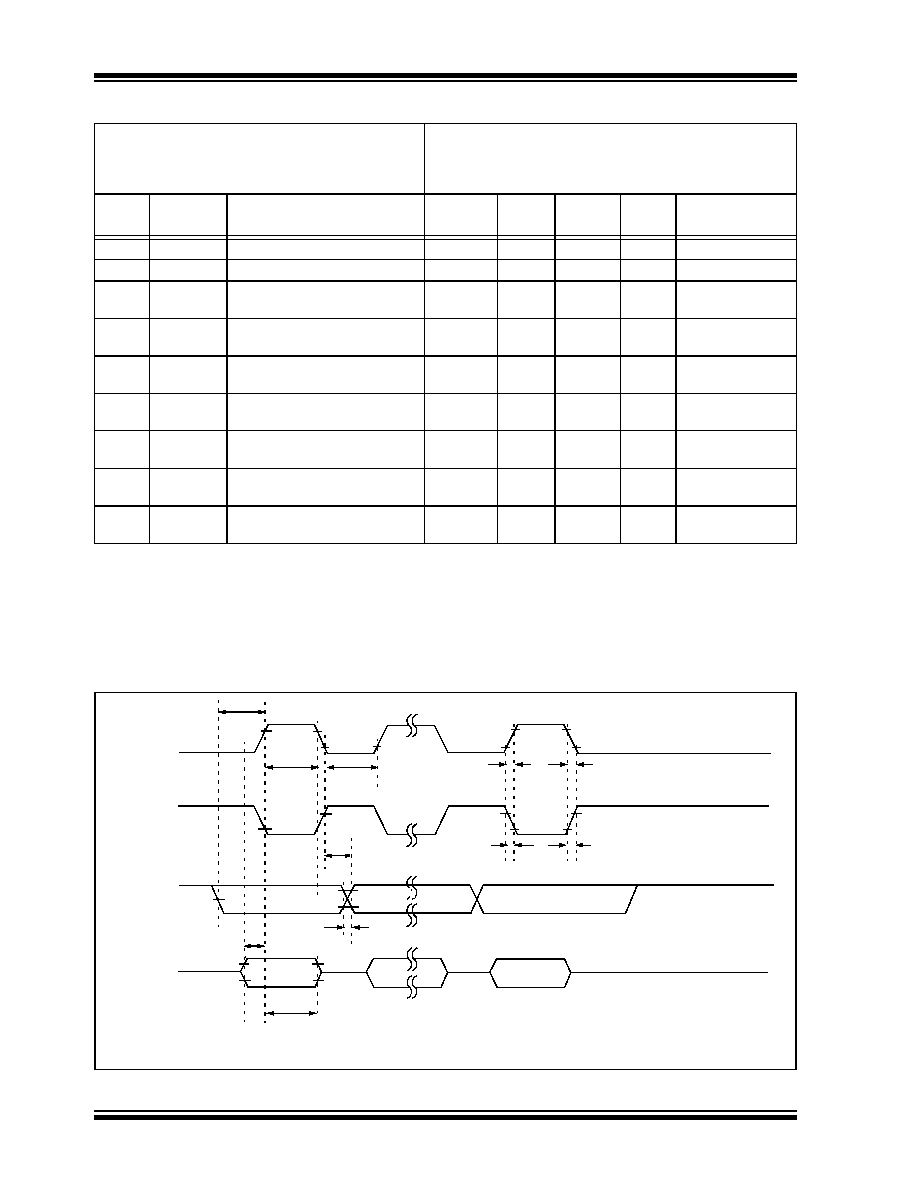
FIGURE 23-15:
SPI MODULE MASTER MODE (CKE =1) TIMING CHARACTERISTICS
TABLE 23-30: SPI MASTER MODE (CKE = 0) TIMING REQUIREMENTS
AC CHARACTERISTICS
Standard Operating Conditions: 2.5V to 5.5V
(unless otherwise stated)
Operating temperature
-40°C
TA +85°C for Industrial
-40°C
TA +125°C for Extended
Param
No.
Symbol
Characteristic(1)
Min
Typ(2)
Max
Units
Conditions
SP10
TscL
SCKX Output Low Time(3)
TCY/2
—
ns
SP11
TscH
SCKX Output High Time(3)
TCY/2
—
ns
SP20
TscF
SCKX Output Fall Time(4
—
ns
See parameter
SP21
TscR
SCKX Output Rise Time(4)
—
ns
See parameter
SP30
TdoF
SDOX Data Output Fall Time(4)
—
ns
See parameter
SP31
TdoR
SDOX Data Output Rise Time(4)
—
ns
See parameter
SP35
TscH2doV,
TscL2doV
SDOX Data Output Valid after
SCKX Edge
—
30
ns
SP40
TdiV2scH,
TdiV2scL
Setup Time of SDIX Data Input
to SCKX Edge
20
—
ns
SP41
TscH2diL,
TscL2diL
Hold Time of SDIX Data Input
to SCKX Edge
20
—
ns
Note 1:
These parameters are characterized but not tested in manufacturing.
2:
Data in “Typ” column is at 5V, 25°C unless otherwise stated. Parameters are for design guidance only and
are not tested.
3:
The minimum clock period for SCKx is 100 ns. Therefore, the clock generated in Master mode must not
violate this specification.
4:
Assumes 50 pF load on all SPI pins.
SCKX
(CKP = 0)
SCKX
(CKP = 1)
SDOX
SDIX
SP36
SP30,SP31
SP35
MSb
MSb In
Bit 14 - - - - - -1
LSb In
Bit 14 - - - -1
LSb
Note: Refer to Figure 23-3 for load conditions.
SP11
SP10
SP20
SP21
SP20
SP40
SP41
发布紧急采购,3分钟左右您将得到回复。
相关PDF资料
SFW15R-2STE1
SFW15R-2STE1-FFC/FPC CONN
PIC18F26J11-I/ML
IC PIC MCU FLASH 64K 2V 28-QFN
PIC18F46K20-E/ML
IC PIC MCU FLASH 32KX16 44QFN
PIC24FJ64GA002-I/SO
IC PIC MCU FLASH 64KB 28SOIC
PIC16C711-04/P
IC MCU OTP 1KX14 A/D 18DIP
PIC18LF26K22-I/SP
IC PIC MCU 64KB FLASH 28SPDIP
PIC18F25K80-I/SP
MCU PIC 32KB FLASH 28SDIP
DSPIC33FJ12MC201-I/SS
IC DSPIC MCU/DSP 12K 20SSOP
相关代理商/技术参数
PIC18F45J11-I/PT
功能描述:8位微控制器 -MCU 32KB Flash 4KBRAM 12MIPS nanoWatt RoHS:否 制造商:Silicon Labs 核心:8051 处理器系列:C8051F39x 数据总线宽度:8 bit 最大时钟频率:50 MHz 程序存储器大小:16 KB 数据 RAM 大小:1 KB 片上 ADC:Yes 工作电源电压:1.8 V to 3.6 V 工作温度范围:- 40 C to + 105 C 封装 / 箱体:QFN-20 安装风格:SMD/SMT
PIC18F45J11T-I/ML
功能描述:8位微控制器 -MCU 32KB Flash 4KBRAM 12MIPS nanoWatt RoHS:否 制造商:Silicon Labs 核心:8051 处理器系列:C8051F39x 数据总线宽度:8 bit 最大时钟频率:50 MHz 程序存储器大小:16 KB 数据 RAM 大小:1 KB 片上 ADC:Yes 工作电源电压:1.8 V to 3.6 V 工作温度范围:- 40 C to + 105 C 封装 / 箱体:QFN-20 安装风格:SMD/SMT
PIC18F45J11T-I/PT
功能描述:8位微控制器 -MCU 32KB Flash 4KBRAM 12MIPS nanoWatt RoHS:否 制造商:Silicon Labs 核心:8051 处理器系列:C8051F39x 数据总线宽度:8 bit 最大时钟频率:50 MHz 程序存储器大小:16 KB 数据 RAM 大小:1 KB 片上 ADC:Yes 工作电源电压:1.8 V to 3.6 V 工作温度范围:- 40 C to + 105 C 封装 / 箱体:QFN-20 安装风格:SMD/SMT
PIC18F45J50-I/ML
功能描述:8位微控制器 -MCU Full Spd USB 32KB 4KBRAM nanoWatt RoHS:否 制造商:Silicon Labs 核心:8051 处理器系列:C8051F39x 数据总线宽度:8 bit 最大时钟频率:50 MHz 程序存储器大小:16 KB 数据 RAM 大小:1 KB 片上 ADC:Yes 工作电源电压:1.8 V to 3.6 V 工作温度范围:- 40 C to + 105 C 封装 / 箱体:QFN-20 安装风格:SMD/SMT
PIC18F45J50-I/PT
功能描述:8位微控制器 -MCU Full Spd USB 32KB 4KBRAM nanoWatt
RoHS:否 制造商:Silicon Labs 核心:8051 处理器系列:C8051F39x 数据总线宽度:8 bit 最大时钟频率:50 MHz 程序存储器大小:16 KB 数据 RAM 大小:1 KB 片上 ADC:Yes 工作电源电压:1.8 V to 3.6 V 工作温度范围:- 40 C to + 105 C 封装 / 箱体:QFN-20 安装风格:SMD/SMT
PIC18F45J50T-I/ML
功能描述:8位微控制器 -MCU Full Spd USB 32KB 4KBRAM nanoWatt RoHS:否 制造商:Silicon Labs 核心:8051 处理器系列:C8051F39x 数据总线宽度:8 bit 最大时钟频率:50 MHz 程序存储器大小:16 KB 数据 RAM 大小:1 KB 片上 ADC:Yes 工作电源电压:1.8 V to 3.6 V 工作温度范围:- 40 C to + 105 C 封装 / 箱体:QFN-20 安装风格:SMD/SMT
PIC18F45J50T-I/PT
功能描述:8位微控制器 -MCU Full Spd USB 32KB 4KBRAM nanoWatt RoHS:否 制造商:Silicon Labs 核心:8051 处理器系列:C8051F39x 数据总线宽度:8 bit 最大时钟频率:50 MHz 程序存储器大小:16 KB 数据 RAM 大小:1 KB 片上 ADC:Yes 工作电源电压:1.8 V to 3.6 V 工作温度范围:- 40 C to + 105 C 封装 / 箱体:QFN-20 安装风格:SMD/SMT
PIC18F45K20-E/ML
功能描述:8位微控制器 -MCU 32KB Flash 1536B RAM 25 I/O 8B RoHS:否 制造商:Silicon Labs 核心:8051 处理器系列:C8051F39x 数据总线宽度:8 bit 最大时钟频率:50 MHz 程序存储器大小:16 KB 数据 RAM 大小:1 KB 片上 ADC:Yes 工作电源电压:1.8 V to 3.6 V 工作温度范围:- 40 C to + 105 C 封装 / 箱体:QFN-20 安装风格:SMD/SMT